 Image 1 of 1
Price: Contact Us
Email: sales@esi-technologies.com
Condition: NEW
Location: SKUE5
In Stock: 100
Product Specifications
Memory Density: 1 Gb (Gigabit)
Configuration: Organized internally as 8 banks of 16Mbit x 8 I/Os.
Voltage Requirement: Operates primarily at a standard 1.5V (± 0.075V). Some variants support low-voltage 1.35V profiles.
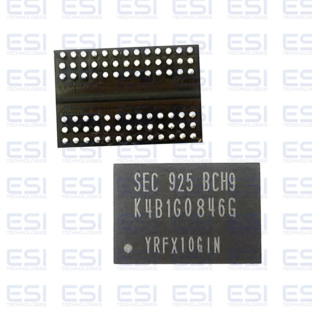
Package Type: 78-ball FBGA (Fine-pitch Ball Grid Array), making it compact for PCB surface mounting.
Material Compliance: Environmentally friendly, lead-free, and halogen-free design.
JEDEC standard 1.5V ± 0.075V Power Supply
VDDQ = 1.5V ± 0.075V
400 MHz fCK for 800Mb/sec/pin, 533MHz fCK for 1066Mb/sec/pin, 667MHz fCK for 1333Mb/sec/pin, 800MHz fCK for 1600Mb/sec/pin 900MHz fCK for 1866Mb/sec/pin
8 Banks
Programmable CAS Latency(posted CAS): 5,6,7,8,9,10,11,13
Programmable Additive Latency: 0, CL-2 or CL-1 clock
Programmable CAS Write Latency (CWL) = 5 (DDR3-800), 6 (DDR3-1066), 7 (DDR3-1333), 8 (DDR3-1600) and 9 (DDR3-1866)
8-bit pre-fetch
Burst Length: 8 (Interleave without any limit, sequential with starting address “000” only), 4 with tCCD = 4 which does not allow seamless read or write [either On the fly using A12 or MRS]
Bi-directional Differential Data-Strobe
Internal(self) calibration : Internal self calibration through ZQ pin (RZQ : 240 ohm ± 1%)
On Die Termination using ODT pin
Average Refresh Period 7.8us at lower than TCASE 85°C, 3.9us at 85°C < TCASE < 95 °C
Asynchronous Reset
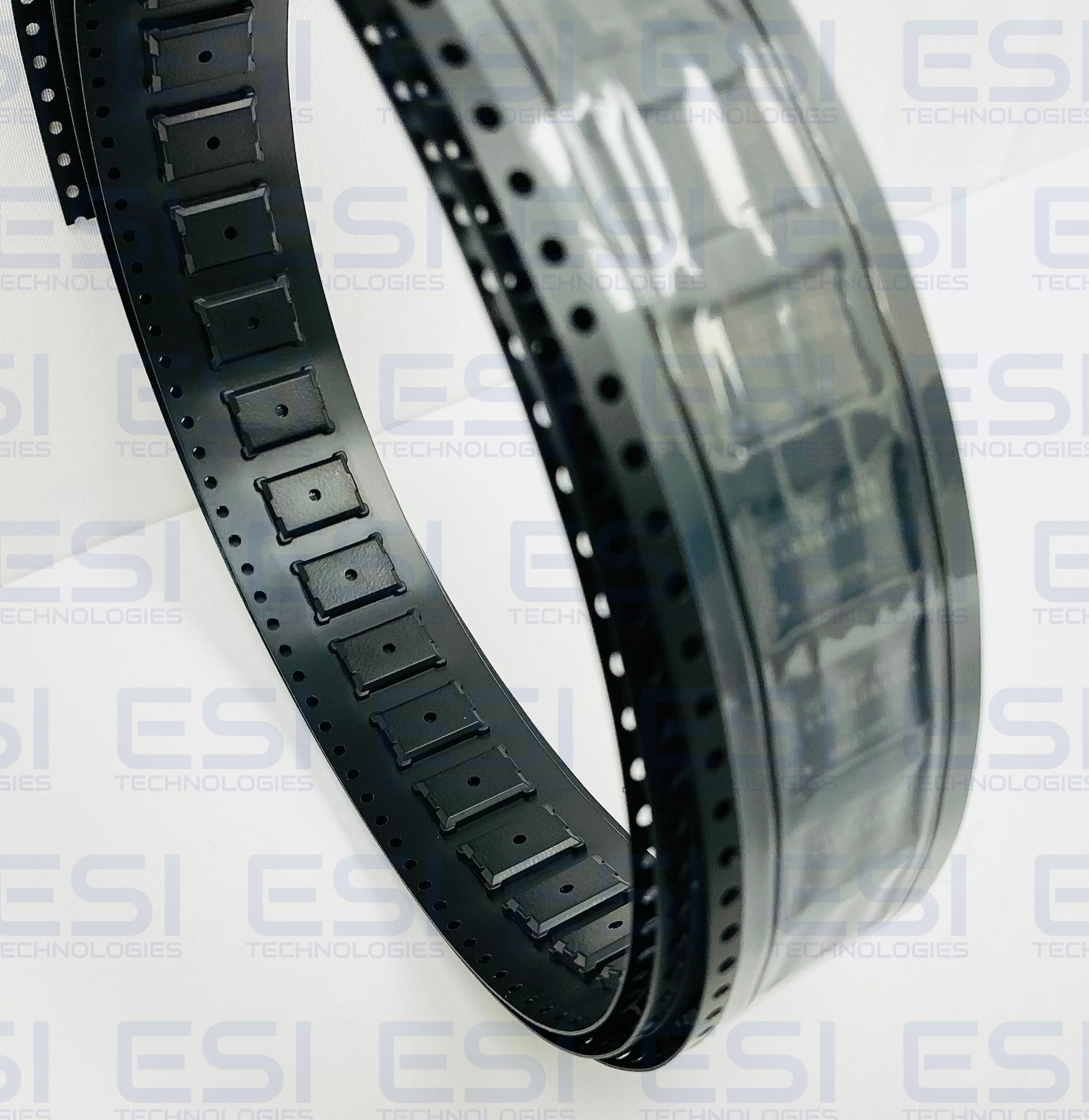
Package : 78 balls FBGA - x4/x8
All of Lead-Free products are compliant for RoHS
All of products are Halogen-free
The Samsung K4B1G0846G-BCH9 is a 1-Gigabit (1Gb) DDR3 SDRAM memory chip organized as 128M × 8 in a BGA package. It belongs to the "G-die" generation is utilized in various data-intensive computing and industrial electronics applications. It is categorized as a specialized Integrated Circuit (IC) used in various electronic devices.
Alternative Part No. K4B1G0846G-BCH9, K4B1G0846G-BCF8, K4B1G0846G-BCK0, K4B1G0846G-HCK0, K4B1G0846G-BCMA
Product Manual
Product Images